A PROPER APPROACH TO SHIELDING
Product consequence is usually most advantageous from a cost, program, grade, and execution perspective to evaluate and execute the proper technique as early as feasible in the project expansion cycle. Add-ons and other “quick” pickles that run later in the scheme are, more frequently than not, non-ideal answers functionally, are of subordinate grade and dependability, and are more expensive than if they had been executed momentarily in operation. A shortage of foresight in the project’s early creation steps usually results in late loads and potentially dissatisfied clients (both internal and external). This issue involves any design, whether analog, digital, electrical, mechanical, etc.
The shielding prices improve the further away it is from separate ICs or small rooms on a PCB. Compared with protecting individual ICs and small areas of a PCB, it costs roughly 10x to watch an entire PCB, 100x to shield a finished product, and 1000x to cover a whole group or chamber. The price is astronomical if shielding of a complete room or building is needed because inappropriate shielding (or no shielding) was executed at lower levels.
A “nested” shielding method is a viable solution. A nested design involves shielding at each of the lowest feasible classes of a product design. For example, shielding is preferably used to:
- Particular ICs/small area of the PCB, obeyed by
- Absolute PCBs, then
- Sub-assemblies, and eventually
- To finish the effects.
A nested shielding process results in the most subordinate general cost to fabricate a quality creation on time and within implementation specifications.
SHIELDING AT THE LOWEST POSSIBLE LEVELS
Shielding at the lowest possible levels (separate ICs, remote areas of the PCB, and the PCB level) creates a lot of sense for several explanations:
- Enclosure shielding does not help attenuate interference between separate ICs found on a PCB, whereas PCB class shielding does help attenuate interference between different ICs.
- From a practical/cost-efficiency class, traditional square shielding technology cannot deliver an effective attenuation version at higher (GHz) commonnesses, whereas PCB level shielding does give this interpretation.
- From a vulnerability standpoint, current ICs, with their ever-shrinking silicon components, more rapid rise times, and inferior noise margins, can perform dependably in the noisy environment they often need to work in just by covering at the PCB level.
- Combining deliberately noisy wireless transmission modules within effects can cause dangerous assumptions to other acute analog and digital elements nearby. This noise can also be mitigated through the help of PCB level shielding.
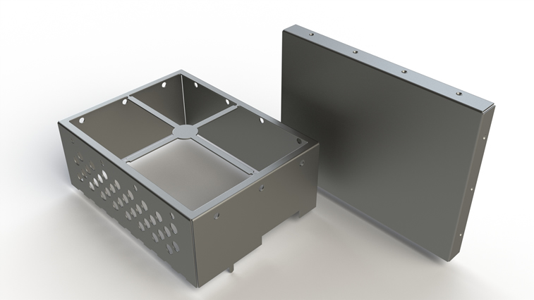
PCB-level security must form an entire six-sided metallic section to deliver the most help. This is achieved by fusing the deposit to a solid foundation plane that lies beneath all the features that require shielding. The ground plane must not have significant slots or spaces to be most helpful. The real-world version of all shielding and land planes is invariably compromised by crevices such as holes for adjustments, indicators, wires, building seams, and the gaps between a shielding can’s bottom plane associations, so whenever feasible, these items should be bypassed.